
The ESP8266 offers a generous number of GPIO pins, which means you don’t have to worry about juggling or multiplexing your IO pins. However, it is important to pay attention to the pinout and read it carefully to ensure proper usage.

It is essential to note that the pinout reference provided here pertains specifically to the widely used 30-pin ESP8266 NodeMCU development board.
While not all ESP8266 development boards have the same pin configuration, it is important to understand that each individual pin functions in the same manner across different development boards.
Parts Required
| Component Name | Buy Now |
| ESP8266 NodeMCU CP2102 | Amazon |
ESP8266 Peripherals and I/O
The ESP8266 NodeMCU is equipped with a total of 17 GPIO pins, conveniently placed on the pin headers on both sides of the development board. These pins can be assigned various peripheral tasks, offering flexibility in their usage.
| 1 ADC channel | 1 channel of 10-bit precision SAR ADC |
| 2 UART interfaces | 2 UART interfaces with with support for flow control |
| 4 PWM outputs | 4 PWM pins to control things like motor speed or LED brightness |
| 2 SPI and 1 I2C interfaces | Two SPI and one I2C interfaces for connecting various sensors and peripherals |
| I2S interface | One I2S interface for adding sound to your project |
One remarkable feature of the ESP8266 is its pin multiplexing capability, enabling multiple peripherals to share a single GPIO pin. This means that a single GPIO pin can perform functions such as I2C, I2S, UART, PWM, and more. For detailed information about the ESP8266, it is recommended to refer to the datasheet.
ESP8266 Pinout
The ESP8266 NodeMCU features a total of 30 pins, organized in a convenient manner where pins with similar functionality are grouped together. Here is the pinout:

Now, let’s examine each of the ESP8266 pins individually and explore their respective functions.
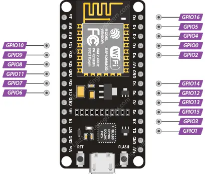
GPIO Pins
The ESP8266 NodeMCU is equipped with 17 GPIO (General Purpose Input/Output) pins that offer flexibility in terms of their functionality. By programming the appropriate registers, each GPIO pin can be assigned different functions. Additionally, these pins can be configured with internal pull-up or pull-down resistors, or set to high impedance mode.
Which ESP8266 GPIOs are safe to use?
While the ESP8266 offers a wide range of GPIO pins with different functionalities, it’s important to note that not all pins are equally safe to use for every project. The table provided below outlines the GPIO pins that are considered safe to use, as well as those that should be used with caution:
 Your top priority pins. They are perfectly safe to use.
 Pay close attention because their behavior, particularly during boot, can be unpredictable. Use them only when absolutely necessary.
 It is recommended that you avoid using these pins.
| Label | GPIO | Safe to use? | Reason |
| D0 | GPIO16 | | HIGH at boot, used to wake up from deep sleep |
| D1 | GPIO5 | | |
| D2 | GPIO4 | | |
| D3 | GPIO0 | | connected to FLASH button, boot fails if pulled LOW |
| D4 | GPIO2 | | HIGH at boot, boot fails if pulled LOW |
| D5 | GPIO14 | | |
| D6 | GPIO12 | | |
| D7 | GPIO13 | | |
| D8 | GPIO15 | | Required for boot, boot fails if pulled HIGH |
| RX | GPIO3 | | Rx pin, used for flashing and debugging |
| TX | GPIO1 | | Tx pin, used for flashing and debugging |
| CLK | GPIO6 | | Connected to Flash memory |
| SDO | GPIO7 | | Connected to Flash memory |
| CMD | GPIO11 | | Connected to Flash memory |
| SD1 | GPIO8 | | Connected to Flash memory |
| SD2 | GPIO9 | | Connected to Flash memory |
| SD3 | GPIO10 | | Connected to Flash memory |
| A0 | ADC0 | | Analog input pin, cannot be configured as output |
It’s recommended to exercise caution when using the GPIO pins mentioned under the “Caution Advised” category, as they may have specific functions or limitations that could affect their usage in certain scenarios.

ADC Pins
The ESP8266 is equipped with a 10-bit precision SAR ADC, allowing it to detect 1024 discrete analog levels. This means it can convert input voltages ranging from 0 to 3.3V (the operating voltage) into integer values ranging from 0 to 1024. Consequently, the resolution is 3.3 volts divided by 1024 units, which equals 0.0032 volts (or 3.2 mV) per unit.
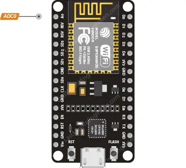
The ADC functionality can be used to perform two specific measurements, although they cannot be executed simultaneously:
- Measuring the power supply voltage of VDD3P3 (Pin 3 and Pin 4).
- Measuring the input voltage of A0.
Please note that these measurements cannot be conducted concurrently due to the limitations of the ADC.
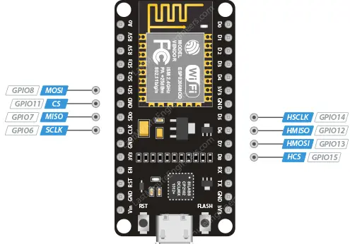
SPI Pins
The ESP8266 incorporates two SPIs (SPI and HSPI) that can operate in both slave and master modes. These SPI interfaces provide support for various general-purpose SPI features, including:
- Four timing modes for SPI format transfer.
- Clock frequencies of up to 80 MHz and the availability of divided clocks at 80 MHz.
- A FIFO (First-In-First-Out) buffer with a capacity of up to 64 bytes.
I2C Pins
Although the ESP8266 does not have dedicated hardware I2C pins, it can still support I2C communication using a technique called ‘bitbanging’. The ESP8266 is capable of achieving speeds comparable to Arduino-level I2C communication.
By default, GPIO4 (SDA) and GPIO5 (SCL) are designated as the I2C pins to provide compatibility with existing Arduino code, libraries, and sketches.
However, if needed, you can utilize any other two GPIO pins as I2C pins by calling wire.begin(SDA, SCL) in the Arduino IDE.

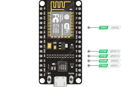
UART Pins
The ESP8266 is equipped with two UART interfaces: UART0 and UART2. These interfaces support asynchronous communication protocols such as RS232 and RS485, with a maximum baud rate of 4.5 Mbps.
For communication purposes, UART0 (TXD0, RXD0, RST0, and CTS0 pins) is used.
UART1 (TXD1 pin) only provides a data transmit signal and is commonly used for printing logs or diagnostic purposes.
PWM Pins
The ESP8266 offers the capability to generate pulse width modulated (PWM) outputs on all of its GPIO pins, ranging from GPIO0 to GPIO15.
With a 10-bit resolution, the PWM signal on the ESP8266 provides fine control over the pulse width. Additionally, the PWM frequency can be adjusted within a range of 1000 μs to 10000 μs, equivalent to a frequency range of 100 Hz to 1 kHz.
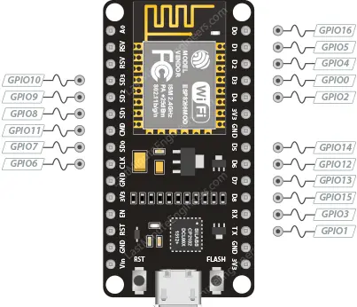
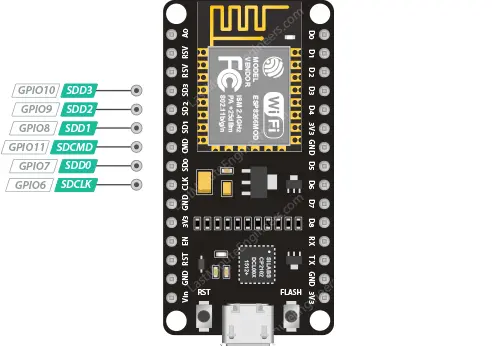
SDIO Pins
The ESP8266 is equipped with a single SDIO (Secure Digital Input/Output Interface) specifically designed for connecting SD cards. It supports both SDIO v1.1 (4-bit 25 MHz) and SDIO v2.0 (4-bit 50 MHz) for efficient data transfer.
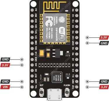
Power Pins
The ESP8266 provides several power-related pins for its operation:
- VIN: This pin allows direct power supply to the ESP8266 and its peripherals when using a regulated 5V power source.
- 3V3: This pin outputs a regulated 3.3V voltage from the on-board voltage regulator, capable of delivering up to 600mA of current.
- GND: This pin serves as the ground connection for the ESP8266 and should be connected to the ground of the power supply or other components for proper operation.
Interrupt Pins
The ESP8266 allows the configuration of GPIO pins to function as interrupts, providing a way to respond to specific events or changes in input. However, it’s important to note that GPIO16 cannot be configured as an interrupt pin.
Control Pins
The ESP8266 includes several control pins that serve specific functions:
EN (CH_PD or Chip Power Down) Pin: This pin is used to enable or disable the ESP8266. By default, it is pulled high, enabling the chip. When pulled low, the chip is disabled.
RST (Reset) Pin: The RST pin is responsible for resetting the ESP8266. It is pulled high by default. To initiate a reset, momentarily pull the pin down to ground. This action is equivalent to pressing the on-board RST button.
FLASH Pin: The FLASH pin is utilized by the ESP8266 to determine whether to boot into the bootloader. If the pin is held low during power-up, the chip enters bootloading mode. This functionality is similar to pressing the on-board FLASH button.
WAKE Pin: The WAKE pin is specifically used to wake the ESP8266 from deep sleep mode, allowing it to resume operation.

Related article
- Step-by-Step Tutorial: Installing ESP8266 Board in Arduino IDE
- Mastering ESP8266 GPIO Interrupts: Arduino IDE Configuration Tips
- Complete Guide: ESP8266 Over The Air (OTA) Programming with Arduino IDE


Wow, this is incredibly helpful! I’ve been struggling to keep track of all the pinouts on my ESP8266 boards. Your reference chart has saved me so much time and frustration. Thank you for putting this together!